

Printed circuit boards (PCBs) are at the heart of nearly every electronic device, from smartphones to industrial machinery. Ensuring their quality and reliability is essential for manufacturers who want to avoid costly failures and maintain customer trust. Electronics manufacturing inspection systems have become indispensable tools in this process, providing automated, accurate, and consistent quality checks throughout production. This article explores how these advanced solutions are transforming PCB manufacturing, the types of inspection technologies available, and how companies can leverage them for superior results.
As the complexity of PCBs increases, so does the need for robust inspection processes. Automated inspection systems not only catch defects that might be missed by manual checks but also help manufacturers scale up production without compromising quality. For those interested in the future of autonomous quality control, understanding the current landscape of inspection technology is a crucial first step.
Why Automated Inspection Matters in PCB Production
Manual inspection has long been a part of electronics manufacturing, but it comes with limitations. Human inspectors can miss subtle defects, especially as board designs become denser and more intricate. Automated inspection systems address these challenges by providing:
- Consistency: Machines apply the same criteria to every board, reducing the risk of human error.
- Speed: Automated systems can inspect hundreds or thousands of boards per hour, keeping pace with modern production lines.
- Traceability: Inspection data is logged and can be analyzed for process improvements or compliance audits.
- Comprehensive defect detection: Advanced imaging and analysis catch issues like solder bridges, missing components, and misalignments that may escape the human eye.
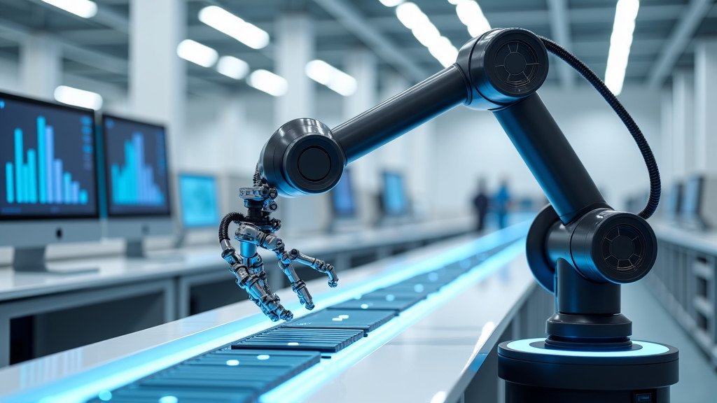
By integrating these systems, manufacturers can reduce rework, lower scrap rates, and deliver higher-quality products to market. This is especially important as consumer expectations rise and regulatory standards become more stringent.
Types of Inspection Technologies in Electronics Manufacturing
There are several key technologies used in electronics manufacturing inspection systems, each suited to different stages of PCB production and types of defects:
Automated Optical Inspection (AOI)
AOI uses high-resolution cameras and sophisticated image processing algorithms to examine PCBs for surface defects, incorrect component placement, and soldering issues. AOI is fast, non-contact, and ideal for catching visible problems early in the process.
Automated X-ray Inspection (AXI)
AXI systems penetrate the board to inspect solder joints beneath components like BGAs (ball grid arrays) that are invisible to optical systems. This technology is essential for detecting hidden defects such as voids, insufficient solder, or bridging under chips.
In-Circuit Testing (ICT)
ICT checks the electrical performance of assembled boards by probing test points. It verifies that each component is correctly placed and functioning, ensuring that the board will operate as intended.
Solder Paste Inspection (SPI)
SPI systems measure the volume and placement of solder paste before components are mounted. Accurate solder paste application is critical for reliable solder joints, and SPI helps prevent defects before they occur.
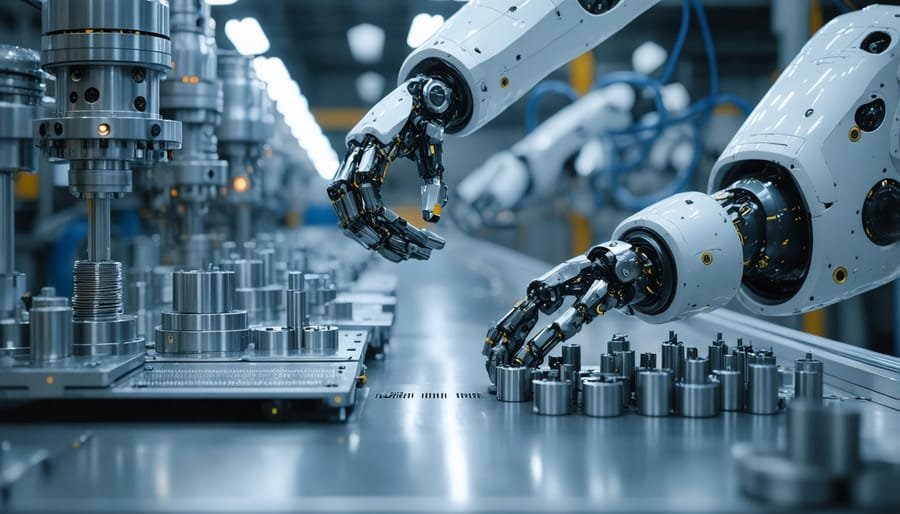
Emerging solutions, such as vision transformers for industrial use, are pushing the boundaries of what automated inspection can achieve, enabling even more precise and adaptive quality control.
Integrating Inspection Systems into the Manufacturing Workflow
The effectiveness of inspection technology depends on how well it is integrated into the broader manufacturing process. Leading manufacturers use a combination of AOI, AXI, SPI, and ICT at different stages to create a layered defense against defects. Key integration strategies include:
- Inline inspection: Placing inspection stations directly on the production line for real-time feedback and immediate corrective action.
- Data-driven process improvement: Using inspection results to identify recurring issues and adjust upstream processes, such as stencil design or pick-and-place programming.
- Continuous monitoring: Leveraging continuous monitoring practices to ensure ongoing quality and quickly detect deviations from standards.
For companies exploring digital transformation, integrating inspection data with manufacturing execution systems (MES) and analytics platforms can unlock new levels of efficiency and traceability.
AI and Machine Learning in Modern Inspection Solutions
Artificial intelligence is rapidly enhancing the capabilities of electronics manufacturing inspection systems. Machine learning algorithms can learn from vast datasets of PCB images, enabling systems to identify subtle or previously unseen defects. Benefits of AI-driven inspection include:
- Higher detection accuracy: AI can distinguish between true defects and acceptable variations, reducing false positives and unnecessary rework.
- Adaptive learning: Systems improve over time as they process more boards and feedback, keeping pace with evolving product designs.
- Support for manual inspectors: Solutions like wearable AI for manual inspection support provide real-time guidance and verification, blending human expertise with digital precision.
As AI becomes more integrated into inspection workflows, manufacturers can expect even greater consistency and insight from their quality control processes.
Best Practices for Maximizing Inspection Effectiveness
To get the most value from inspection technology, manufacturers should follow these best practices:
- Deploy multiple inspection methods at critical points in the process to catch a wide range of defects.
- Regularly calibrate and maintain inspection equipment to ensure accuracy.
- Train staff to interpret inspection data and respond effectively to alerts.
- Continuously review inspection results to drive process improvements and reduce recurring issues.
- Stay informed about new technologies, such as augmented reality in quality audits, that can further enhance quality assurance.
By treating inspection as a strategic investment rather than a cost center, companies can improve yield, reduce warranty claims, and strengthen their reputation for quality.
Common Challenges and How to Overcome Them
While the benefits of automated inspection are clear, manufacturers may encounter challenges such as:
- High initial investment: Advanced systems can require significant upfront costs, but the long-term savings from reduced defects and rework often justify the expense.
- Integration complexity: Ensuring that inspection systems communicate effectively with other factory equipment and software can be challenging. Choosing solutions with open interfaces and strong vendor support is key.
- Keeping pace with technology: As inspection technology evolves, ongoing training and periodic upgrades are necessary to maintain optimal performance.
Manufacturers who proactively address these challenges position themselves for long-term success in a competitive market.
FAQ
What are the main benefits of using automated inspection in PCB manufacturing?
Automated inspection delivers consistent, high-speed quality checks, reduces human error, and provides detailed data for process improvement. It helps manufacturers catch defects early, lower scrap rates, and ensure reliable products reach customers.
How does AI improve electronics manufacturing inspection systems?
AI enhances defect detection by learning from large datasets, reducing false positives, and adapting to new product designs. It can also support manual inspectors with real-time feedback, increasing overall inspection accuracy and efficiency.
Can inspection systems be integrated with other manufacturing software?
Yes, modern inspection solutions often feature open interfaces for integration with manufacturing execution systems (MES), analytics platforms, and other factory software. This enables real-time data sharing, traceability, and process optimization.